 |   |
I was born in a little town
Zvenigorod near Moscow, Russia (Soviet Union) on July
11, 1962. Then I went to kindergarten, then to elementary...
and to middle... and to high school.
[Pictured above is Novo-Shikhovo village, 5 miles from
Zvenigorod, where I lived for the first 20 years of my life.
The picture was taken in 1972. The place has not changed
much since... well, all empty space visible in this picture
is covered with auto-garages, private shacks and villas now] |  | 
| |
Eventually (in 1979) I entered
Moscow Steel and Alloys Institute (main building is
pictured on the left) where I studied at the Department of
Semiconducor Materials and Devices until graduated with a
Master of Science degree in 1985. |  | 
| |
Since graduation I worked as a staff researcher at
P.N. Lebedev Physical Institute (FIAN, main building is
pictured on the left), Moscow, Russia. While I had been
working there, Soviet Union had collapsed, the Cold War had
ended and you know the rest... |  |  
| |
In August 1992, I entered the
Science and Engineering of Materials Ph.D. Program at
Arizona State University from which I successfully
graduated in December 1995. Continued there as a post-doc
until May 1998. |  |  | |
In June 1998 joined Philips Electron Optics in Eindhoven,
The Netherlands. Now it's called
FEI Electron Optics. | 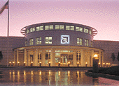 | 
| |
In January 2001 joined
Advanced Micro Devices in Sunnyvale, California. | | | |
I'm married to Alla V.
Sidorova (Shikalova). My daughter,
Anna, was born on November 18, 1986. My son,
Georgy, was born on February 15, 1999. |
|
|